← Microsquirt ECU Wiring Diagram: Optimize Your Engine’s Performance Megasquirt microsquirt ecu w/ 30" wiring harness (microsqrt3 ... Transmitter Wiring Diagram: Easy Setup for Radio & Audio Gear! transmitter / receiver bluetooth 5.1 dac spdif 24bit 96khz usb file ... →
If you are looking for Browse you've came to the right page. We have 25 Images about Browse like What is a Wafer in VLSI - VLSIFacts, silicon wafer - Brewer Science and also Browse. Here it is:
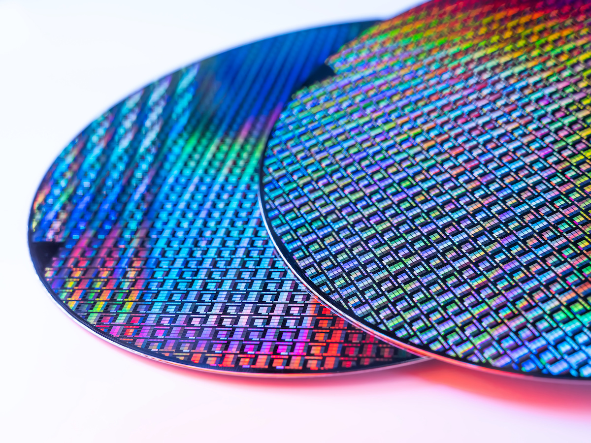
Browse
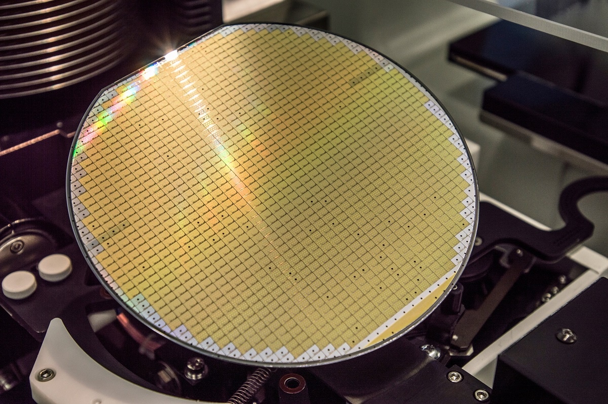 www.st.com
Browse
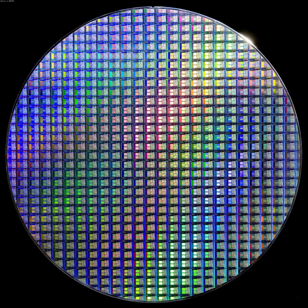
Semiconductor-Wafer-Processing – Tismo – The Design & Engineering Firm
 www.tismotech.com
Semiconductor-Wafer-Processing – Tismo – The Design & Engineering Firm
Simple Silicon Wafer Icon. Vector. 26381158 Vector Art At Vecteezy
Simple silicon wafer icon. Vector. 26381158 Vector Art at Vecteezy
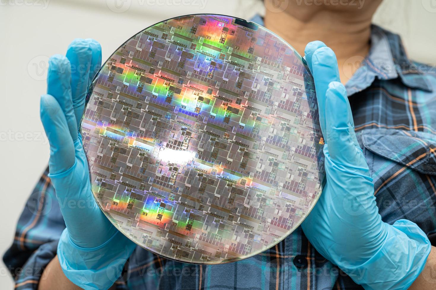
Silicon Wafer For Manufacturing Semiconductor Of Integrated Circuit
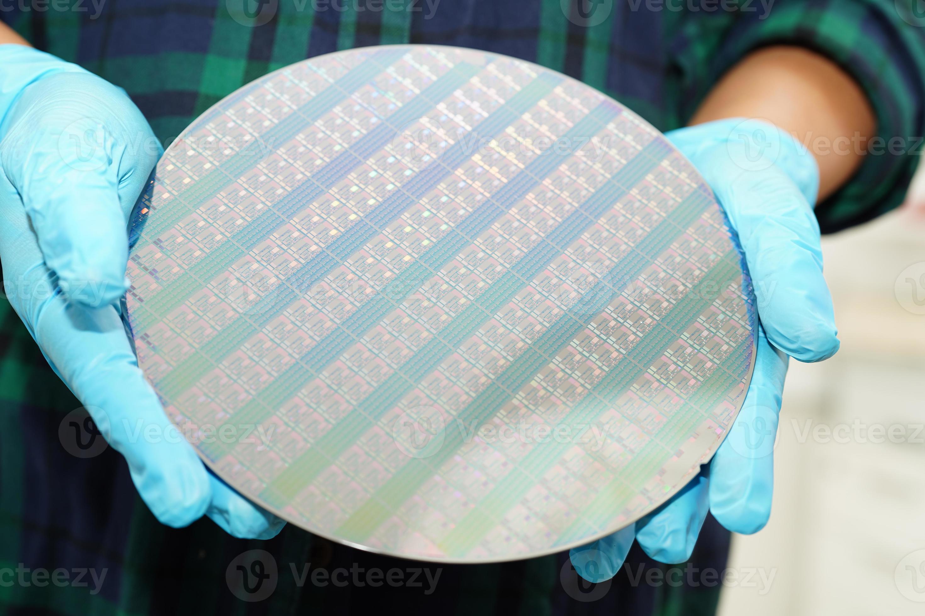 www.vecteezy.com
Silicon wafer for manufacturing semiconductor of integrated circuit ...
Despite 2023 Slump, Wafer Fab Equipment Revenue Will Recover
 www.electronicspecifier.com
Despite 2023 slump, wafer fab equipment revenue will recover
Buy 1pcs 12-inch Wafer Lithography Silicon Wafer Semiconductor
 bahamas.desertcart.com
Buy 1pcs 12-inch Wafer Lithography Silicon Wafer semiconductor ...
Modern Silicon Wafer Icon Or Semiconductor Vector Image
Modern silicon wafer icon or semiconductor Vector Image
4 6 8 Polegada De Silício Wafer Circuito Integrado Sem Cortes Geek Toy
 pt.aliexpress.com
4 6 8 Polegada de Silício Wafer Circuito Integrado Sem Cortes Geek Toy ...
Choosing The Right Wafer Material For Your Needs
-p-1080.jpg) www.waferworld.com
www.waferworld.com
Choosing the Right Wafer Material for Your Needs
Silicon Wafer - Brewer Science
 www.brewerscience.com
silicon wafer - Brewer Science
Accelerating Sustainable Semiconductors With ‘Multielement Ink
 newscenter.lbl.gov
Accelerating Sustainable Semiconductors With ‘Multielement Ink ...
Silicon Wafer For Manufacturing Semiconductor Of Integrated Circuit
 www.alamy.com
Silicon wafer for manufacturing semiconductor of integrated circuit ...
Semiconductor Engineering MPM – 02/22/24
 semiengineering.com
Semiconductor Engineering MPM – 02/22/24
Photoresist Processing Of Double Side Polish Wafer
 www.waferworld.com
Photoresist Processing of Double Side Polish Wafer
Electronics | Free Full-Text | A True Process-Heterogeneous Stacked
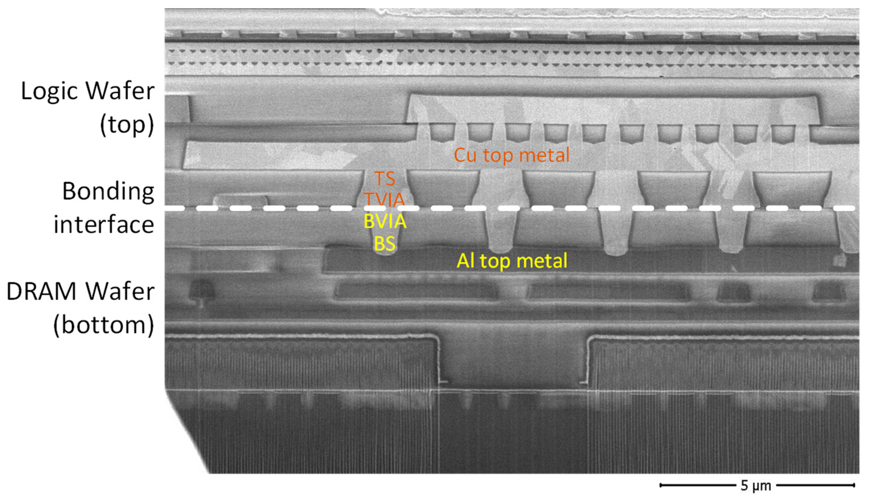 www.mdpi.com
Electronics | Free Full-Text | A True Process-Heterogeneous Stacked ...
A Momentum Contrastive Learning Framework For Low-Data Wafer Defect
 www.mdpi.com
A Momentum Contrastive Learning Framework for Low-Data Wafer Defect ...
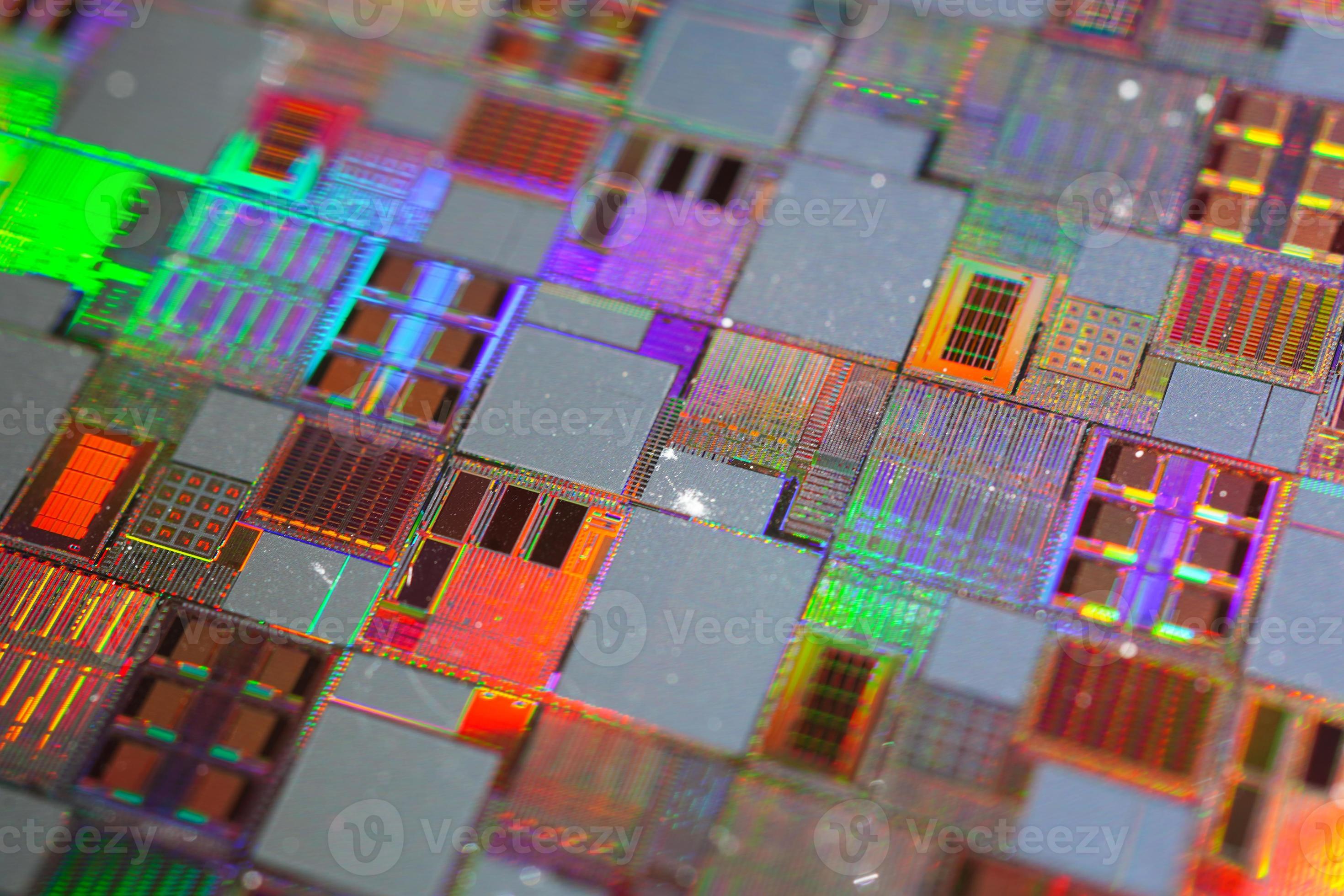
Silicon Wafer For Manufacturing Semiconductor Of Integrated Circuit
 www.vecteezy.com
Silicon wafer for manufacturing semiconductor of integrated circuit ...
Semiconductor Device Manufacturing Process, Challenges And
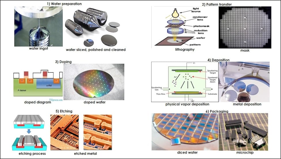 www.renesas.com
Semiconductor Device Manufacturing Process, Challenges and ...
Surface-Finishing Solutions Improve SiC Wafer Efficiency And Cost
 www.powerelectronicsnews.com
Surface-Finishing Solutions Improve SiC Wafer Efficiency and Cost ...
Bosch Reaches Milestone On The Way To Opening New Wafer Fab In Dresden
 www.webwire.com
Bosch reaches milestone on the way to opening new wafer fab in Dresden ...
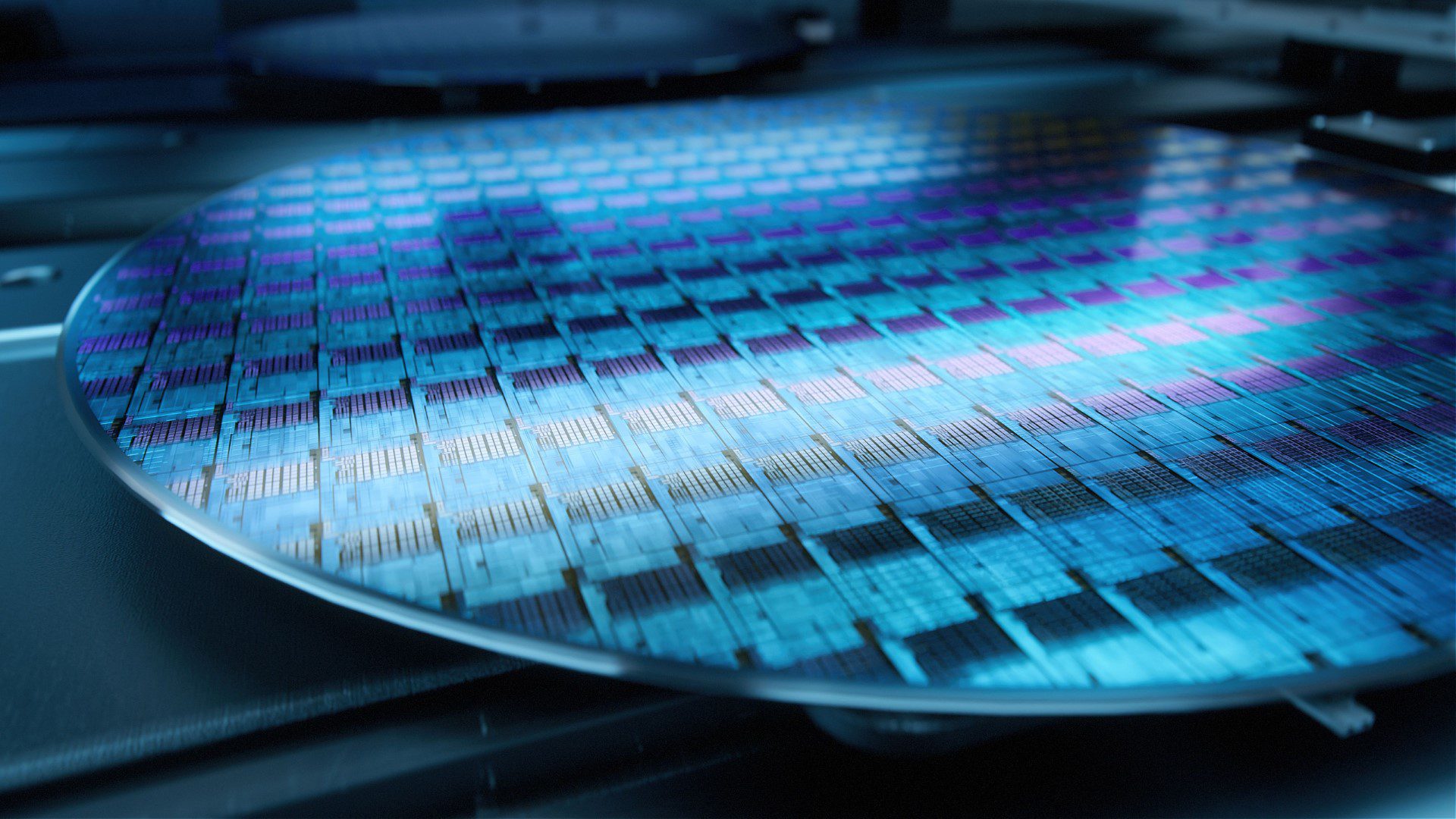
Silicon Wafer For Manufacturing Semiconductor Of Integrated Circuit
 www.vecteezy.com
Silicon wafer for manufacturing semiconductor of integrated circuit ...
TSMC Wil AMD En Nvidia Verleiden Met Prijsdalingen 3nm-wafers - ITdaily.
 itdaily.be
TSMC wil AMD en Nvidia verleiden met prijsdalingen 3nm-wafers - ITdaily.
Advanced Wafer Inspection Solution Launched – Metrology And Quality
 metrology.news
Advanced Wafer Inspection Solution Launched – Metrology and Quality ...
Silicon Wafer For Manufacturing Semiconductor Of Integrated Circuit
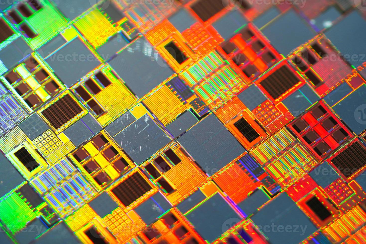 www.vecteezy.com
Silicon wafer for manufacturing semiconductor of integrated circuit ...
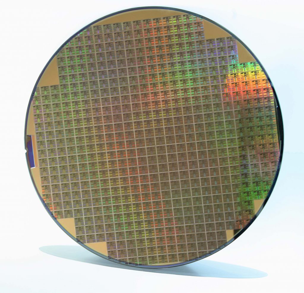
What Is A Wafer In VLSI - VLSIFacts
 vlsifacts.com
What is a Wafer in VLSI - VLSIFacts
Photoresist processing of double side polish wafer. Accelerating sustainable semiconductors with ‘multielement ink .... 4 6 8 polegada de silício wafer circuito integrado sem cortes geek toy ...