← 1971 Honda CL100 Wiring Diagram: Keep Your Vintage Bike Running 1971 honda cl100 scrambler KiCad Highlight Net: The Ultimate Guide for Circuit Design kicad highlight net schematic →
If you are looking for double layer pcb manufacturing you've visit to the right place. We have 25 Pics about double layer pcb manufacturing like What is double-layer PCB and how is it made - complete guide - IBE, What is double-layer PCB and how is it made - complete guide - IBE and also pcb mcrd v3 double layer What is multilayer pcb? definition. Here you go:
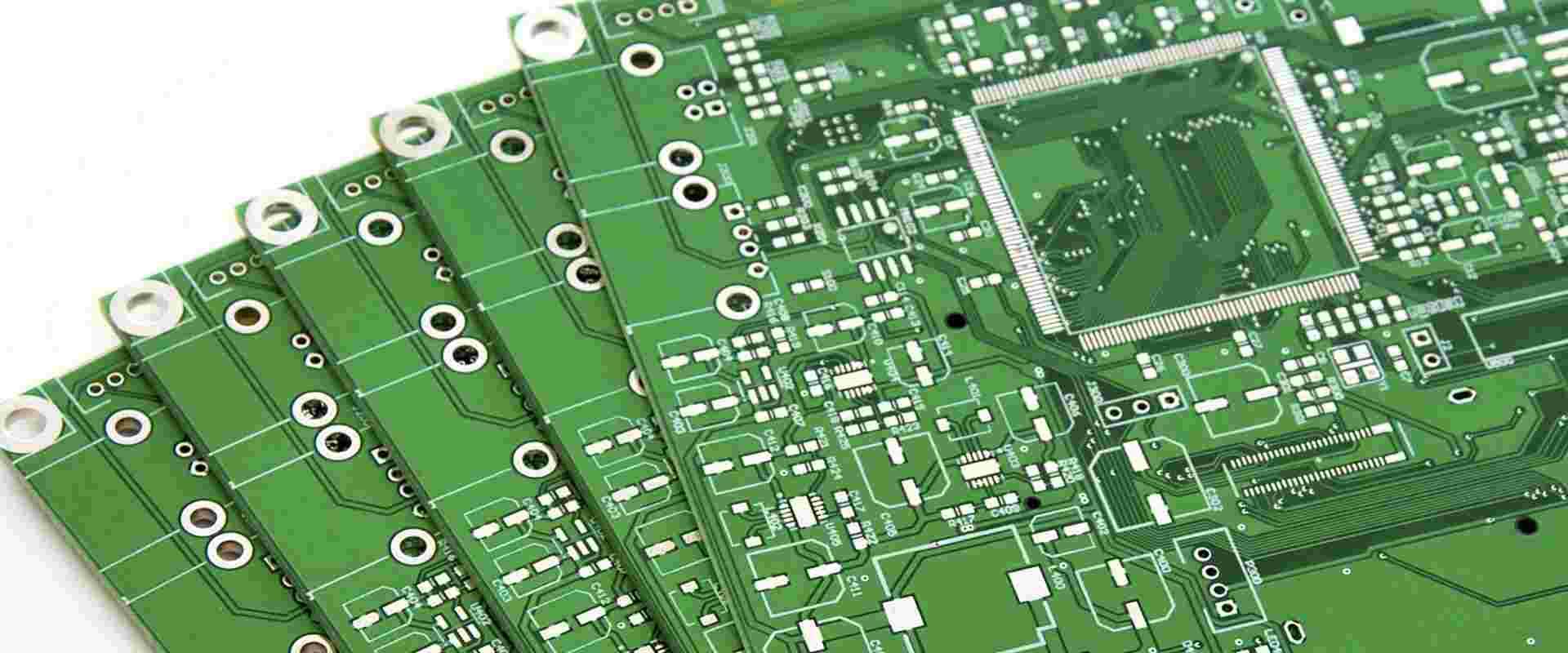
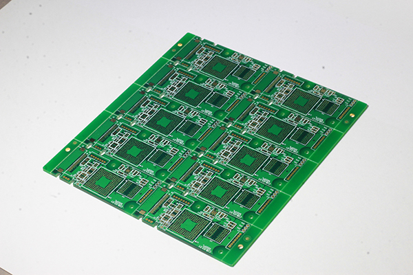
Double Layer Pcb Manufacturing
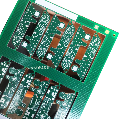 www.oneseine.com
double layer pcb manufacturing
Essential PCB Board Design
_01.jpg) www.wizlogix.com
www.wizlogix.com
Essential PCB Board Design
Tutorial Of 4 Layer PCB Layout, Design And Cost - AES
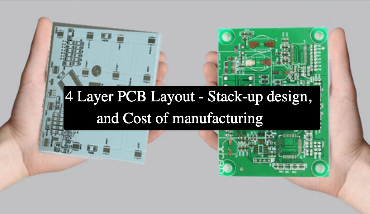 absolutepcbassembly.com
Tutorial of 4 Layer PCB Layout, Design and Cost - AES
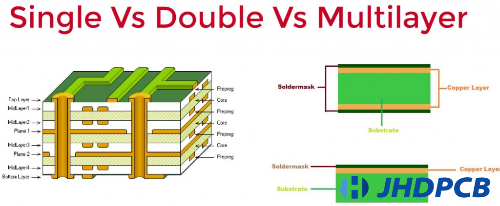
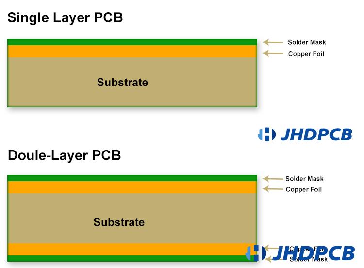
Single & Double Layer PCB - Jhdpcb
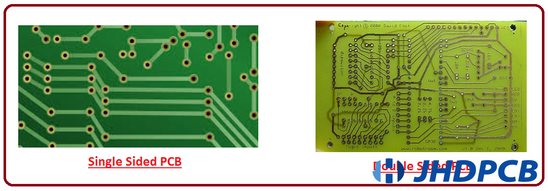 www.jhdpcb.com
Single & Double Layer PCB - Jhdpcb
What Is The Better PCB: 2 Layer Vs 4 Layer PCB?
 www.pcbmay.com
What Is the Better PCB: 2 Layer vs 4 Layer PCB?
What Is Double-layer PCB And How Is It Made - Complete Guide - IBE
 www.pcbaaa.com
What is double-layer PCB and how is it made - complete guide - IBE ...
2-Day Essential And Advanced PCB Design And Layout Techniques For SI
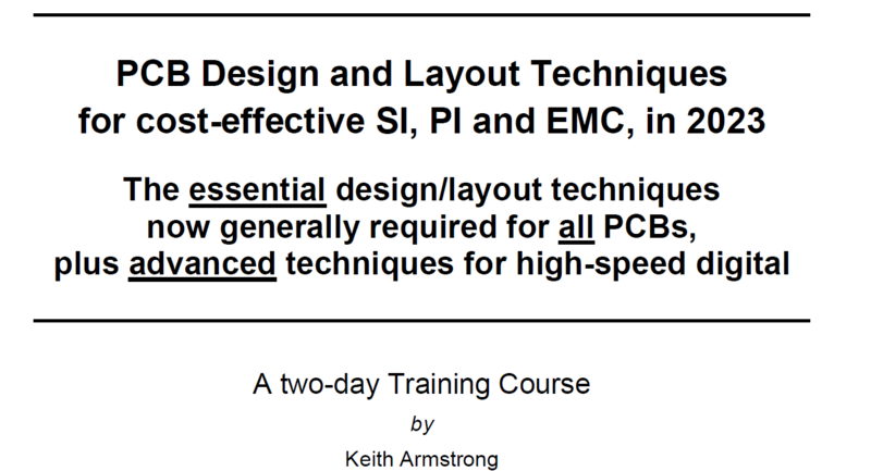 www.emcstandards.co.uk
2-Day Essential and Advanced PCB Design and Layout Techniques for SI ...
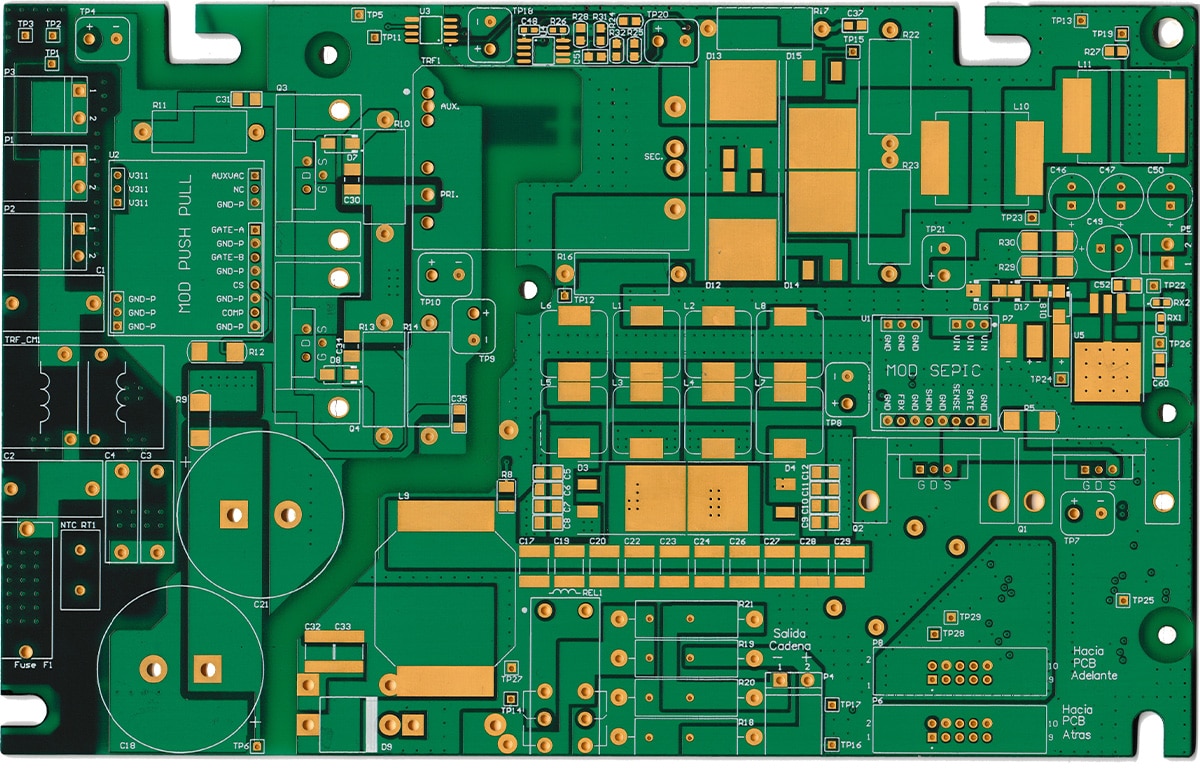
Double Layer PCB For Power Electronics - China Innovative PCB For GPS
 xmdcircuit.en.made-in-china.com
Double Layer PCB for Power Electronics - China Innovative PCB for GPS ...
Pcb Mcrd V3 Double Layer What Is Multilayer Pcb? Definition
 pcbways.pages.dev
pcb mcrd v3 double layer What is multilayer pcb? definition ...
What Is Double-layer PCB And How Is It Made - Complete Guide - IBE
 www.pcbaaa.com
What is double-layer PCB and how is it made - complete guide - IBE ...
Essential Information And Tips For Using Taconic PCB
 pcbassemblymanufacturing.com
Essential information and tips for using Taconic PCB
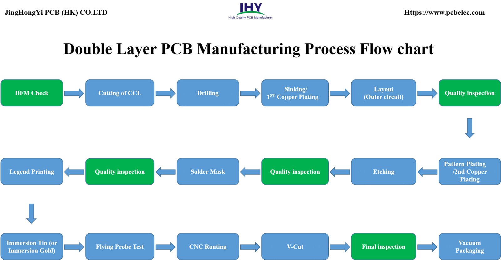
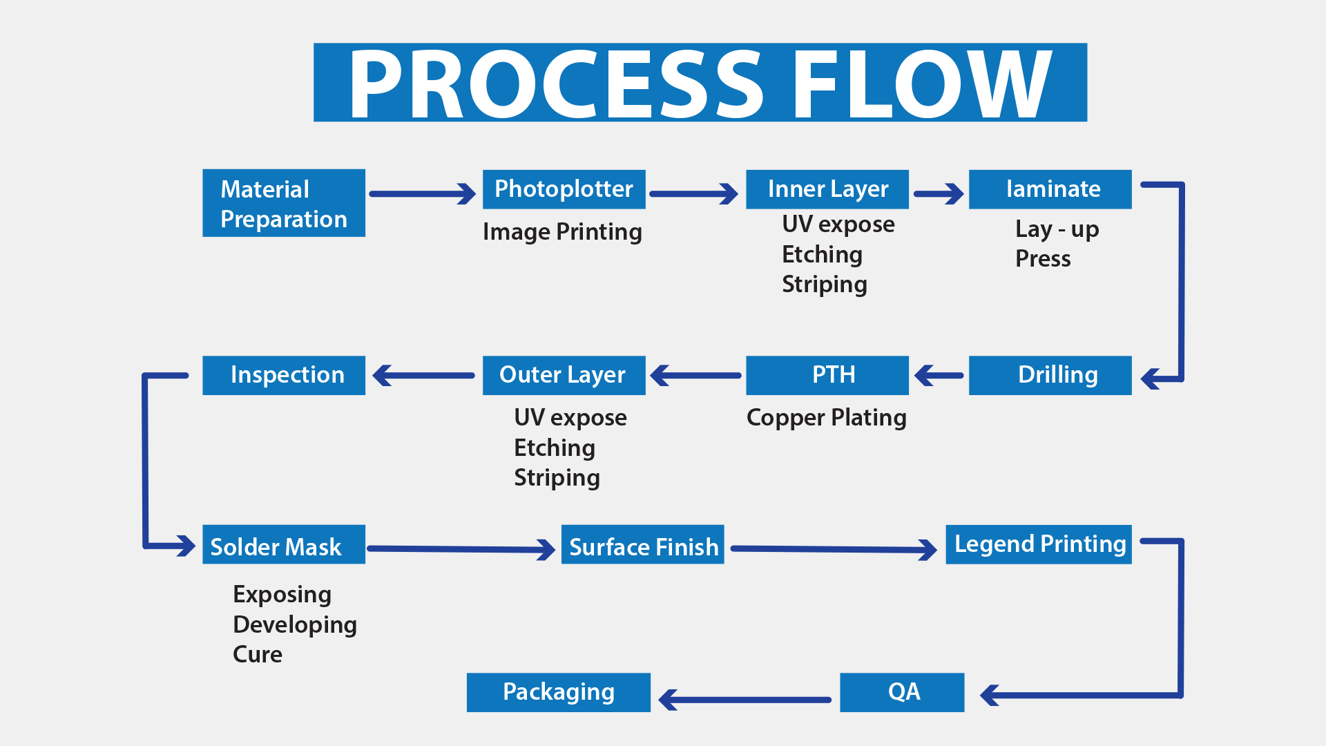
Double-sided PCB Manufacturing Process Flowchart And Step By Step
 www.pcbelec.com
Double-sided PCB Manufacturing Process Flowchart and Step by Step
Typical 2 Layer Pcb Stackup 6-layer Pcb Stackup Design Guidelines
 pcbways.pages.dev
typical 2 layer pcb stackup 6-layer pcb stackup design guidelines
What Is Double-layer PCB And How Is It Made - Complete Guide - IBE
 www.pcbaaa.com
What is double-layer PCB and how is it made - complete guide - IBE ...
Double Layer PCB | Construction And Applications
 circuits-diy.com
Double Layer PCB | Construction And Applications
What Is Double-layer PCB And How Is It Made - Complete Guide - IBE
 www.pcbaaa.com
What is double-layer PCB and how is it made - complete guide - IBE ...
4-Layer PCB Design Guidelines: Key Tips For Success | Viasion
 www.viasion.com
4-Layer PCB Design Guidelines: Key Tips for Success | Viasion
Double Layer Pcb | Printed Circuit Boards | As&r Circuits India Pvt Ltd
 www.plantautomation-technology.com
Double Layer Pcb | Printed Circuit Boards | As&r Circuits India Pvt Ltd
Essential PCB Board Design
_01.jpg) www.wizlogix.com
www.wizlogix.com
Essential PCB Board Design
Single & Double Layer PCB - Jhdpcb
 www.jhdpcb.com
Single & Double Layer PCB - Jhdpcb
Understanding Double Layer PCB - PCBA Manufacturers
 www.pcba-manufacturers.com
Understanding double layer PCB - PCBA Manufacturers
Custom Power Electronics PCB - Bare Printed Circuit Board - Cohen
 www.cohenelec.com
Custom Power Electronics PCB - Bare Printed Circuit Board - Cohen ...
Introduction To Double-sided PCB - The Engineering Projects
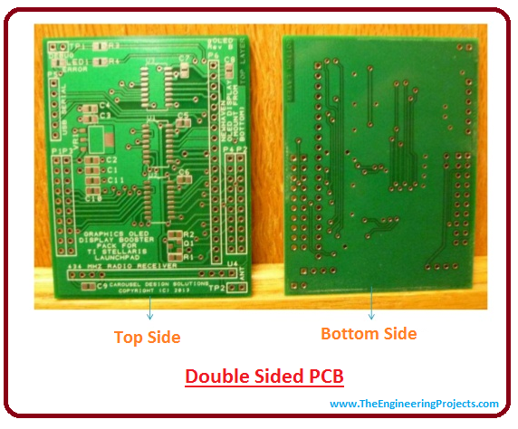 www.theengineeringprojects.com
Introduction to Double-sided PCB - The Engineering Projects
Introduction To Double Layer PCB - The Engineering Projects
 www.theengineeringprojects.com
Introduction to Double Layer PCB - The Engineering Projects
Single & Double Layer PCB - Jhdpcb
 www.jhdpcb.com
Single & Double Layer PCB - Jhdpcb
4-layer pcb design guidelines: key tips for success. Single & double layer pcb. Custom power electronics pcb